Reproducing the RP2350 OTP Power Glitch Attack
Introduction
In this blog post, I walk through my experience replicating the RP2350 OTP hack by Aedan Cullen. I followed the progress of the RP2350 Hacking Challenge (the first edition; Raspberry Pi later launched a second edition), and when the deadline arrived there were multiple solutions. Some were more interesting than others, in my opinion. One I found particularly interesting was Aedan Cullen’s, which relies on glitching the OTP power source. I was keen to try it myself, but I faced some challenges along the way. This post describes my experience attempting to reproduce the attack, including the pitfalls.
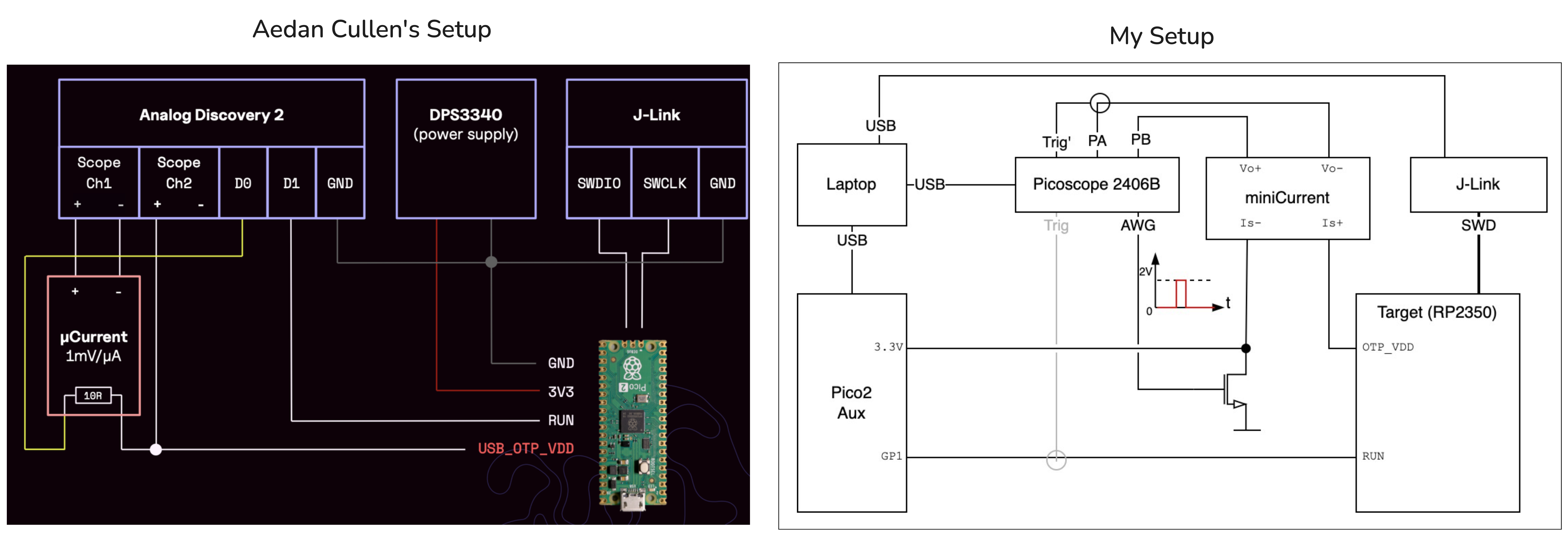
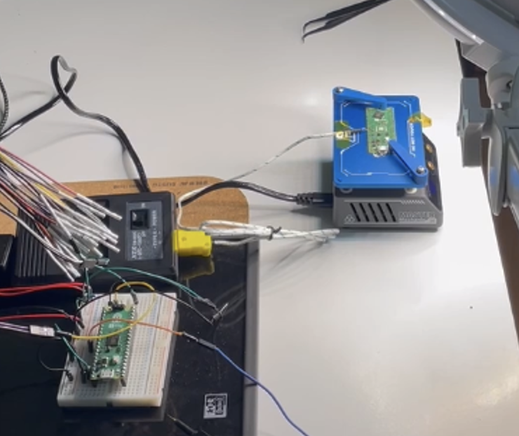
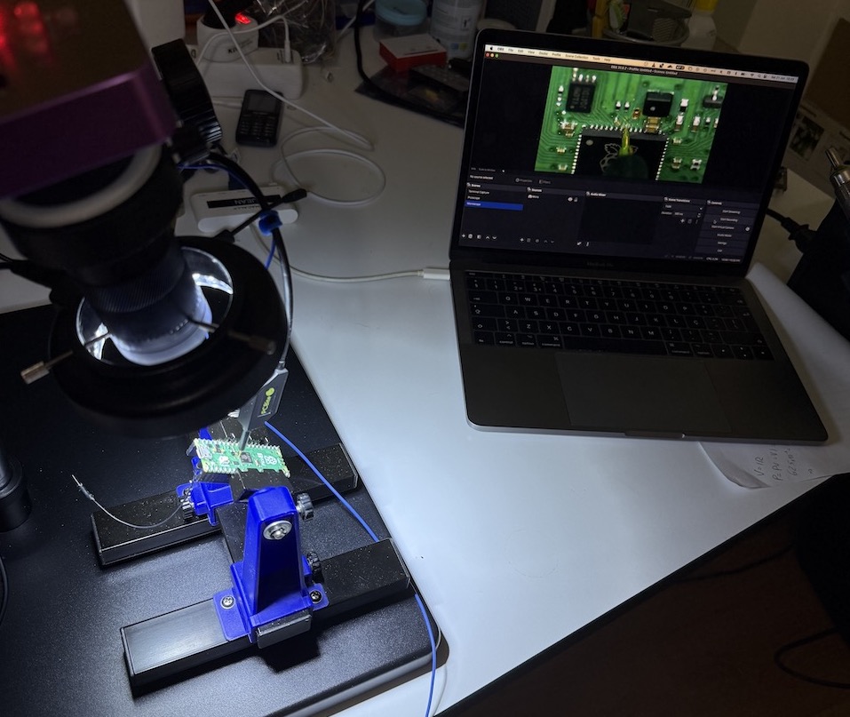
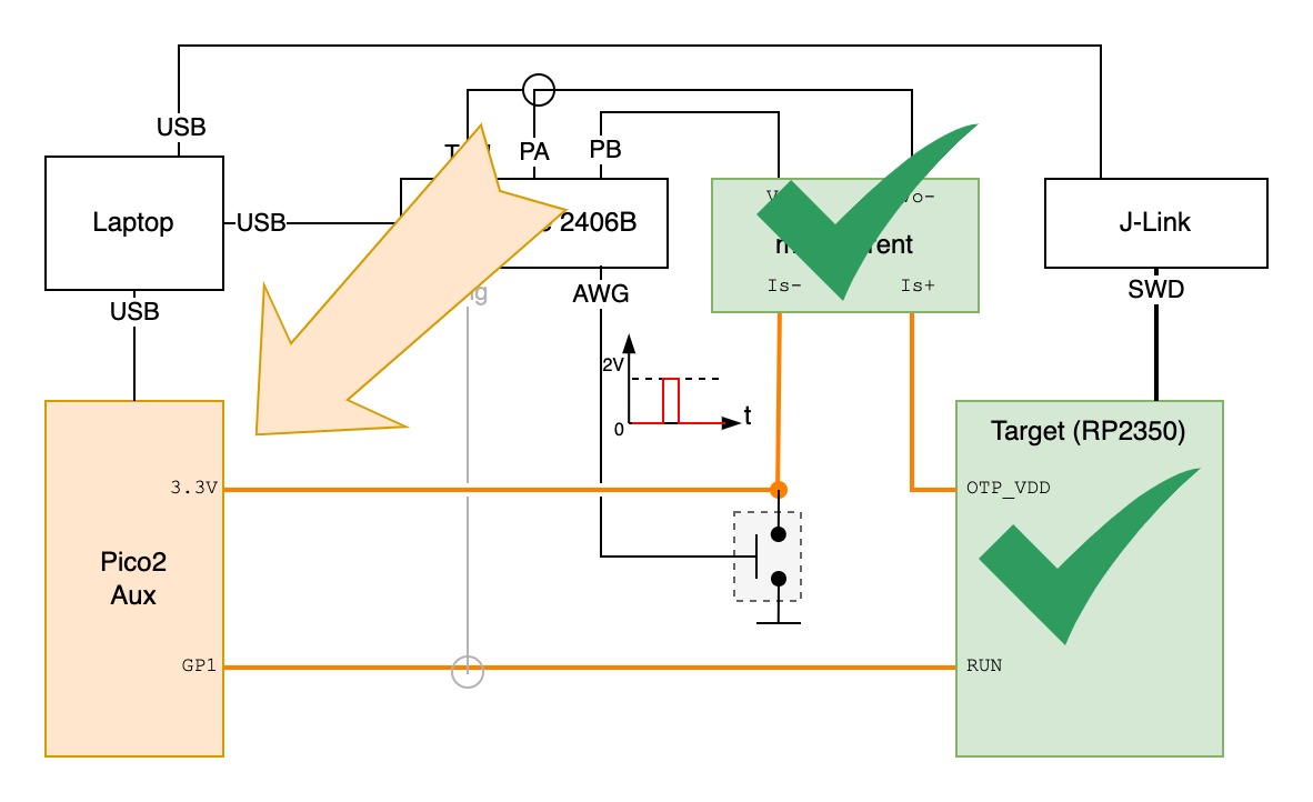
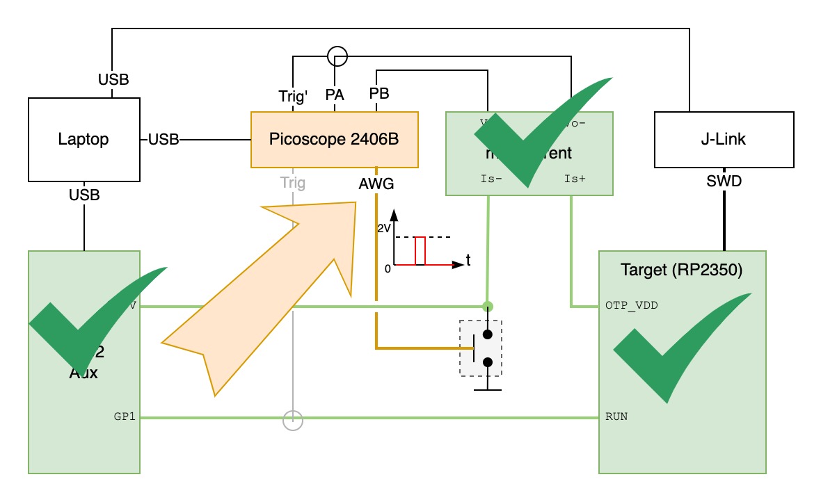
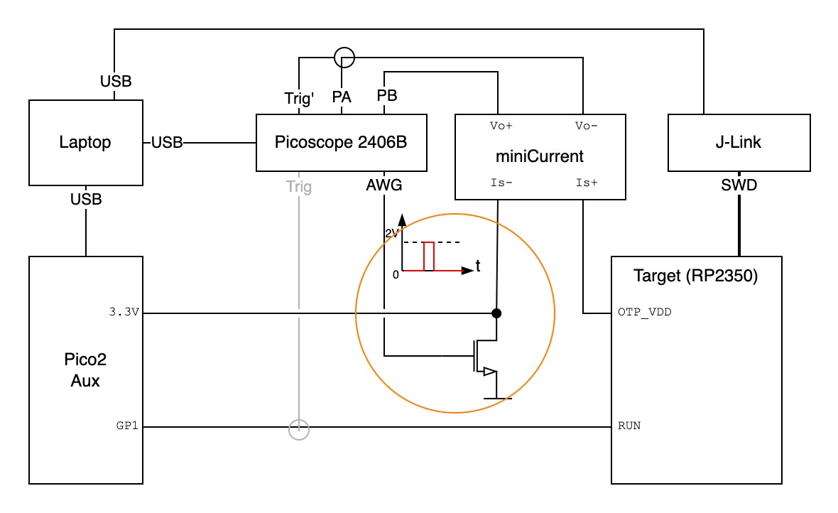
Since the hardware is expensive, it made sense to use our existing lab hardware as much as possible. That led me to perform the attack using different hardware than Aedan used. Both lab setups can be compared in the picture above.
Attack Description
To read the OTP secrets, Aedan’s attack caused the RP2350 to boot the RISC-V cores instead of the ARM. Because the OTP protections and chip security were implemented for the ARM, using the RISC-V makes it possible to read the OTP secrets without those restrictions.
To boot the RISC-V instead of the ARM, Aedan glitched the OTP power pin during a CRITICAL register read, which corrupted the value read to 0x0003033. A value of 0x0003033 means both the RISCV_DISABLE and ARM_DISABLE bits of the CRITICAL register are set, and, coincidentally, when these two bits are set the RP2350 boots the RISC-V. Crazy luck…
Experimental Setup
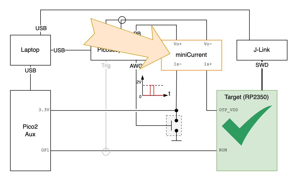
- The Target is the RP2350 of Pico 2 board with secrets inside OTP fuses. To glitch the
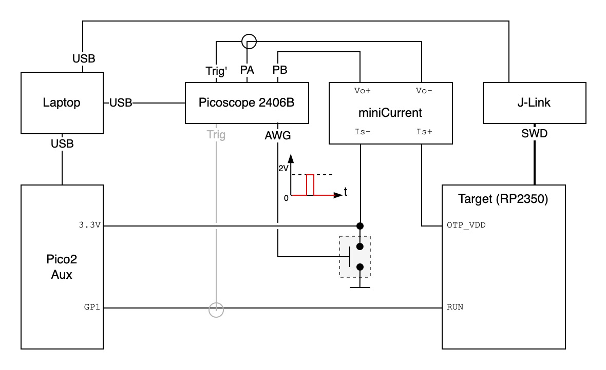
OTP_VDDof the target, we need a way to isolateOTP_VDDfrom the coreVDD. - The miniCurrent is used to measure
OTP_VDDcurrent and locate whenCRITICALregister is read. - The J-Link is the JTAG adapter board.
- The Switch is the glitch circuit, that shorts
OTP_VDDto ground. - The Picoscope 2406B is an analog USB oscilloscope.
- The Pico 2 Aux is an extra Pico 2 board to control the target state (on/off).
- The Laptop has the pico-otp-glitcher code which prepares the different elements and performs the attack automatically.
Table of Contents
Given the long post, I’ve split it into different sections.
- Attack Description
- Preparing the Target
- OTP Read Sequence
- Target Control
- Glitching Signal
- Glitching Circuit
- Automation & Orchestrator
- Debugging & Failed Attempts
- The Real Problem: Jitter
- Conclusion
Preparing the Target
In order to isolate the RP2350 OTP_VDD connection in the Pico 2 board we have to desolder the RP2350, make a cut in the power trace, and resolder it.
Using a hot-air gun is the most practical approach to desolder the RP2350 chip (QFN package). This step shouldn’t be hard at first glance (and from watching some YouTube videos it may look easy). But if you look closely you’ll see several tiny SMD resistors and capacitors around the chip.
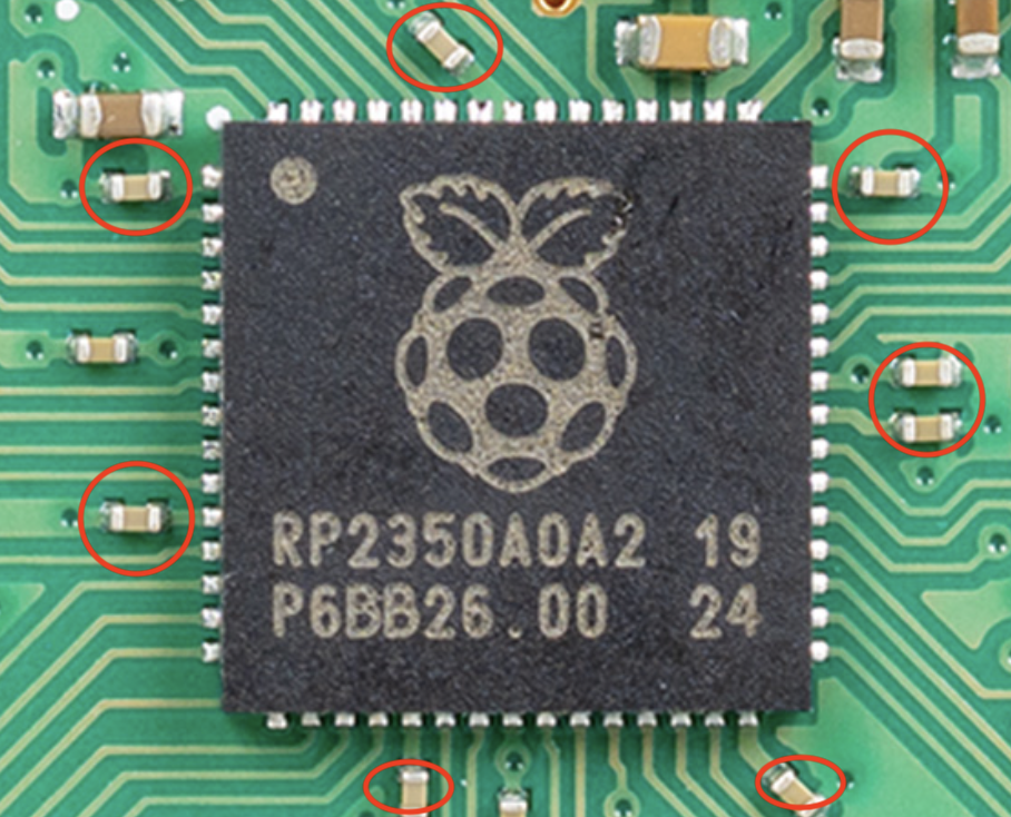
Heating the RP2350 will also easily melt surrounding components’ solder, and a wrong tweezer move can mistakenly disconnect one of these components. I looked into more professional ways of desoldering these types of chips. Apparently, pre-heating the board from the bottom to a certain temperature helps.
To my disappointment this didn’t help much… I probably did something wrong. I resorted to increasing the hot-air gun temperature and desoldering in the simplest way.
One thing that helped was using a reasonable hot-air gun fan speed. A temperature of 250–300ºC and a fan speed of 6–7 worked well on this particular hot-air gun. It’s hard to describe in text, but it felt that a slow fan would not spread the heat enough across the chip and PCB to melt all pads’ solder.
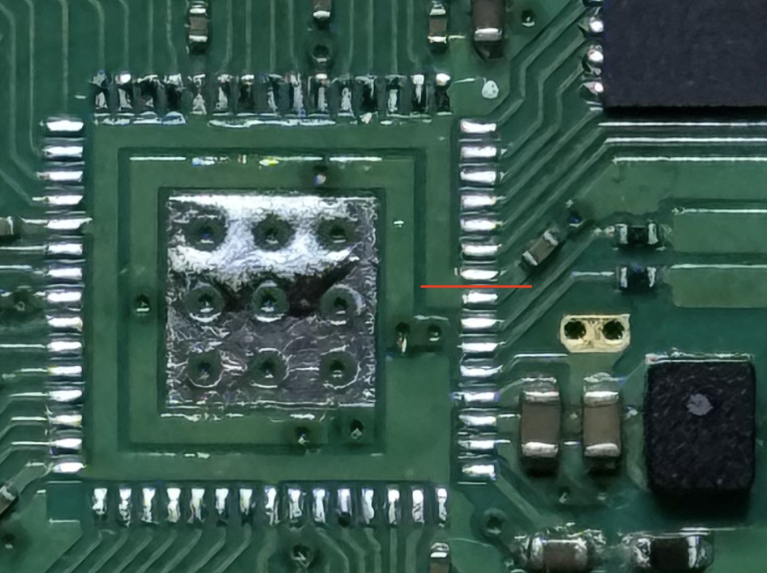
This was new to me. How do you cut a 200 µm trace as illustrated in the picture above? Aedan said he used a knife. I tried twice, and on the second attempt the knife cuts completely removed a PCB pad from the board…
Anyway, will this still work? I don’t need to solder the OTP_VDD pad that is gone, as long as I can connect to the RP2350 OTP_VDD pin… first we have to resolder the RP2350.
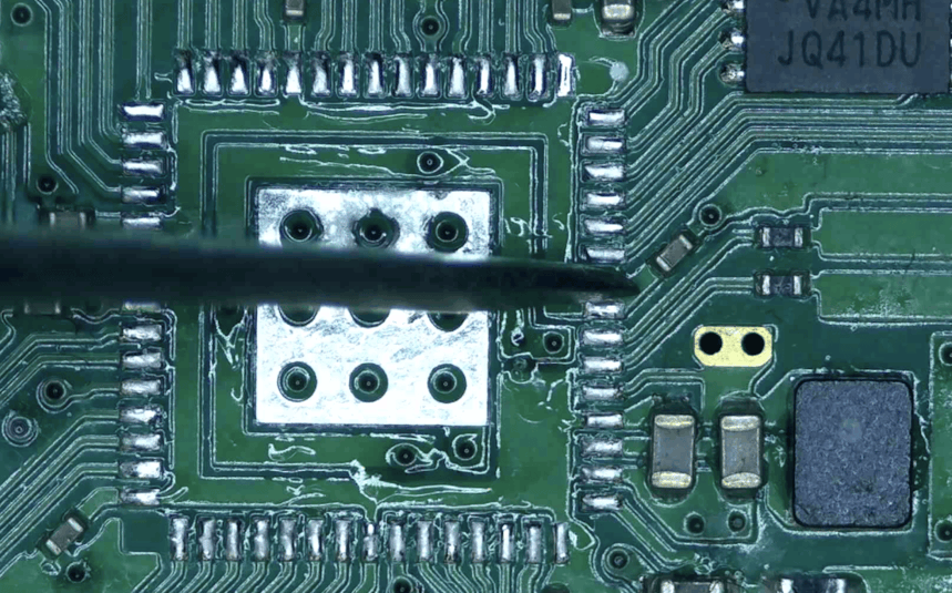
For the resoldering I used the hot-air gun and it was easier. However, after turning it on it didn’t work… 🤨 Can you spot the problem in the picture below? 🤔 You have to zoom in a little.
I inspected the chip-pad soldering and found that the chip was very misaligned; on one side the pins were disconnected or even shorting the wrong pads. Very messy 🤦♂️
OK, but it can be fixed (if the chip still works!). Applying the hot-air gun reflows the solder, which draws the component into precise alignment due to surface tension. Here’s a video showing that effect.
Once it was soldered, I had to confirm it was working. To help connect to the OTP_VDD pin I used a PCbite probe and a digital microscope to see it better.
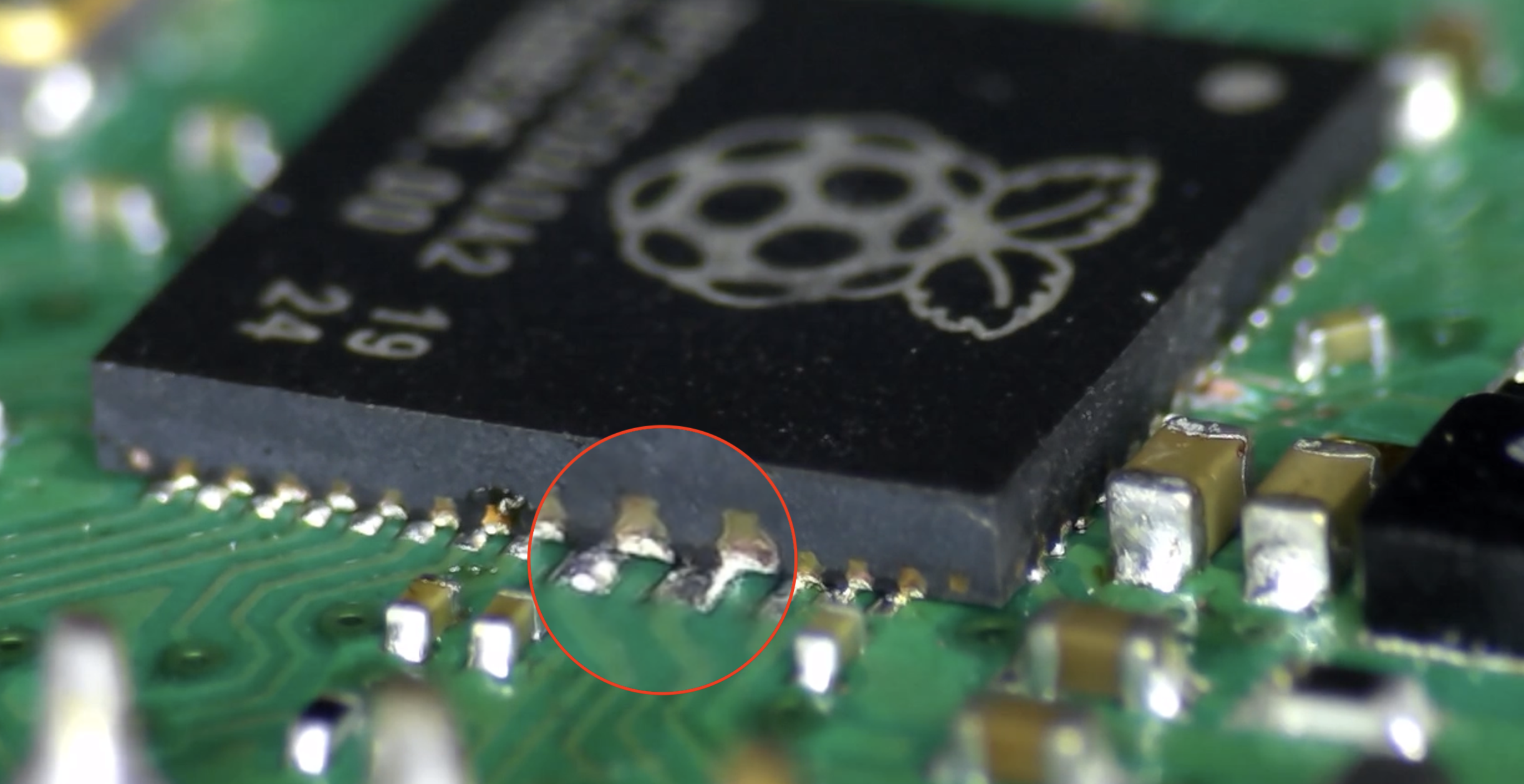
After connecting to the PC and opening the serial port, it showed the “hello world” message. Great, it was working… but not for long. Due to mishandling or the soldering/desoldering process, the chip was damaged and completely stopped working after a while. 😒
Isolating the OTP_VDD got me stuck for a while. I wasn’t sure how to isolate this pin in a way that wouldn’t damage the chip. The process of reworking small-footprint components requires a lot of practice and trial and error. One may still end up with a broken chip unless, in my opinion, specialized hardware is used.
I spent a few weeks away from this project. I thought about fabricating a custom Pico2 PCB, but it was a bit pricey (~80€ from JLCPCB). Then I came across the Hardware Design with RP2350 document from Raspberry Pi, which provides a “minimal board” design shown below.
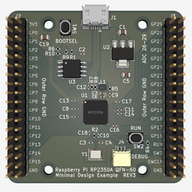
Since it provided KiCad design files, I was able to quickly map the components to JLCPCB basic parts and get an estimate: ~40€ for 2 assembled boards. Not cheap, given that a Pico 2 board costs ~8€. However, I felt stuck and this was a way to resolve the bottleneck, so I decided to go for it.
I only had to make small adjustments to the board:
- Add a pin header for the OTP_VDD
- Change the SMD switches to PDIP ones (cheaper!)
- Remove pin-headers from the fabrication BOM
- Replace the SWD connector to pin-header
- Ensure RP2350A revision A2 is used (newer is patched against this attack)
This made the board cheaper and compatible with what we needed for the attack. The final version is shown below.
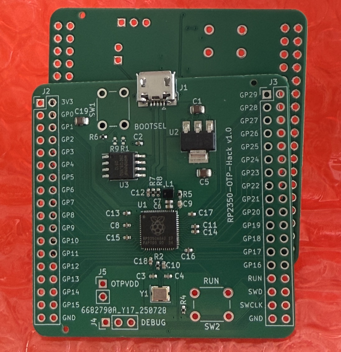
Note: You can find the KiCad project files in the GitHub repo of this post at the end.
I tested that the fabricated board was working as expected. Now that the OTP_VDD is isolated, we have to capture the OTP current and find the pattern of OTP reads from the chip bootstrap.
OTP Read Sequence
In Aedan’s attack, a uCurrent was used to measure the current drawn by the OTP_VDD pin. This is a neat current-to-voltage converter based on a shunt resistor that should be tailored to the scale of currents we’re measuring.
I tried to find this gadget locally but it was either expensive (~$60) or out of stock. So I decided to port the existing project to KiCad and order a PCB + assembly from JLCPCB. As I did this, I learned which parts could be adjusted to squeeze a few euros out: a special inverted LED, an uncommon DP3T slide switch, and a golden-plated “bind post” (the “banana-type” female connector).
I wrote a blog post about this uCurrent variant: miniCurrent Project. Feel free to check it for more details. The final result is the following:
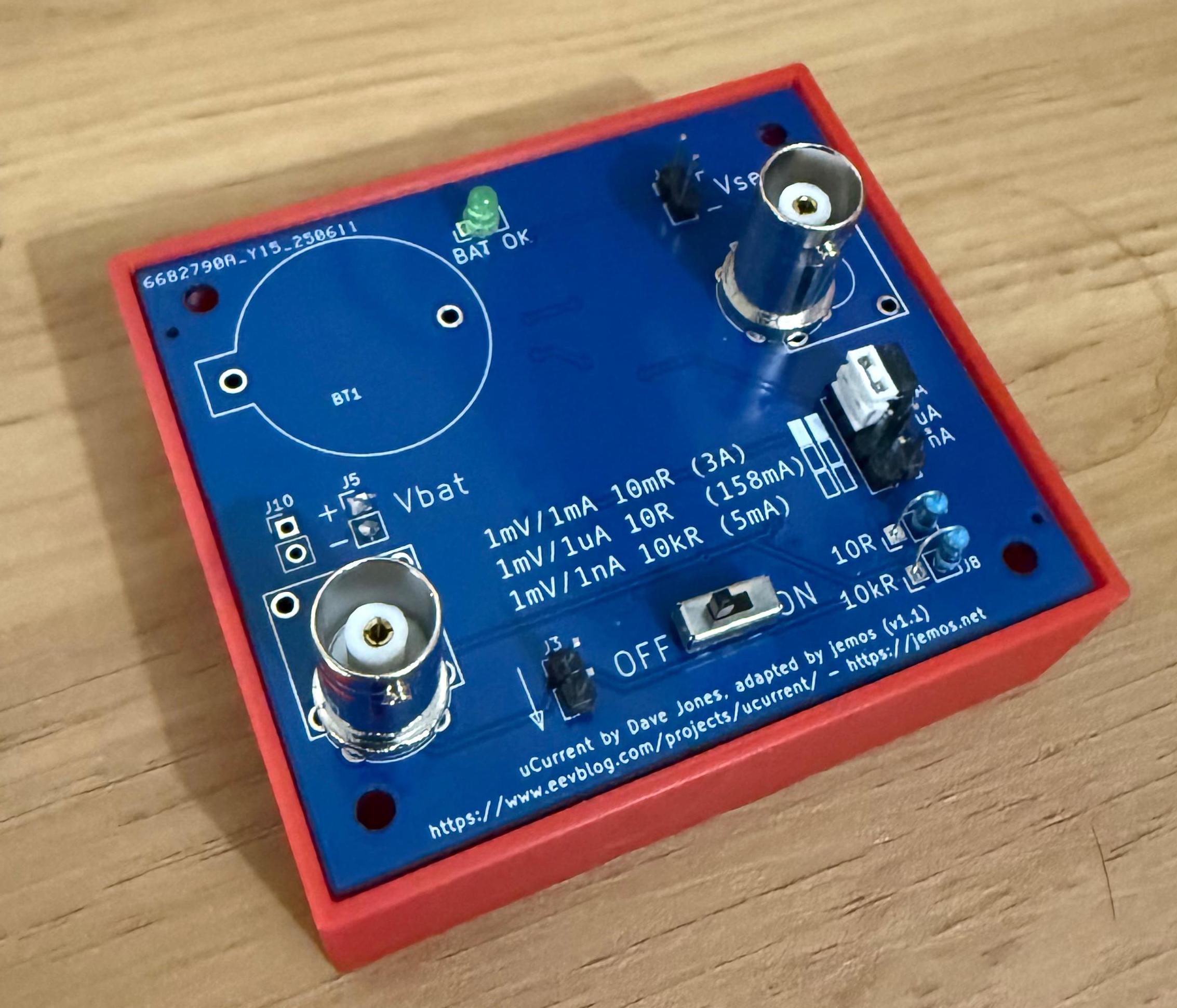
While trying to use the miniCurrent, I made some careless mistakes. This instrument is meant to be connected to a multimeter. You can connect it to an oscilloscope, but you need to consider that the output of the miniCurrent is differential. It has a “virtual” ground to allow negative measurements of current (for example, -120 mV → -120 μA on the 10 Ω scale).
The first mistake was tying the same ground between the miniCurrent and the USB connections. This created a ground loop through the miniCurrent, causing problems. The second mistake was measuring a current above the maximum shunt resistor rating. While nothing smoked, it didn’t smell good 😅
To avoid having to order a new board due to mistakes, I made some tweaks to the original uCurrent design. I’m now using an external 10 kΩ resistor. In addition, I added support for more BNC connectors (an official Wurth Electronics one and a cheap brandless one from AliExpress) and an external battery connector (3×AAA). For more information, see the miniCurrent Project page.
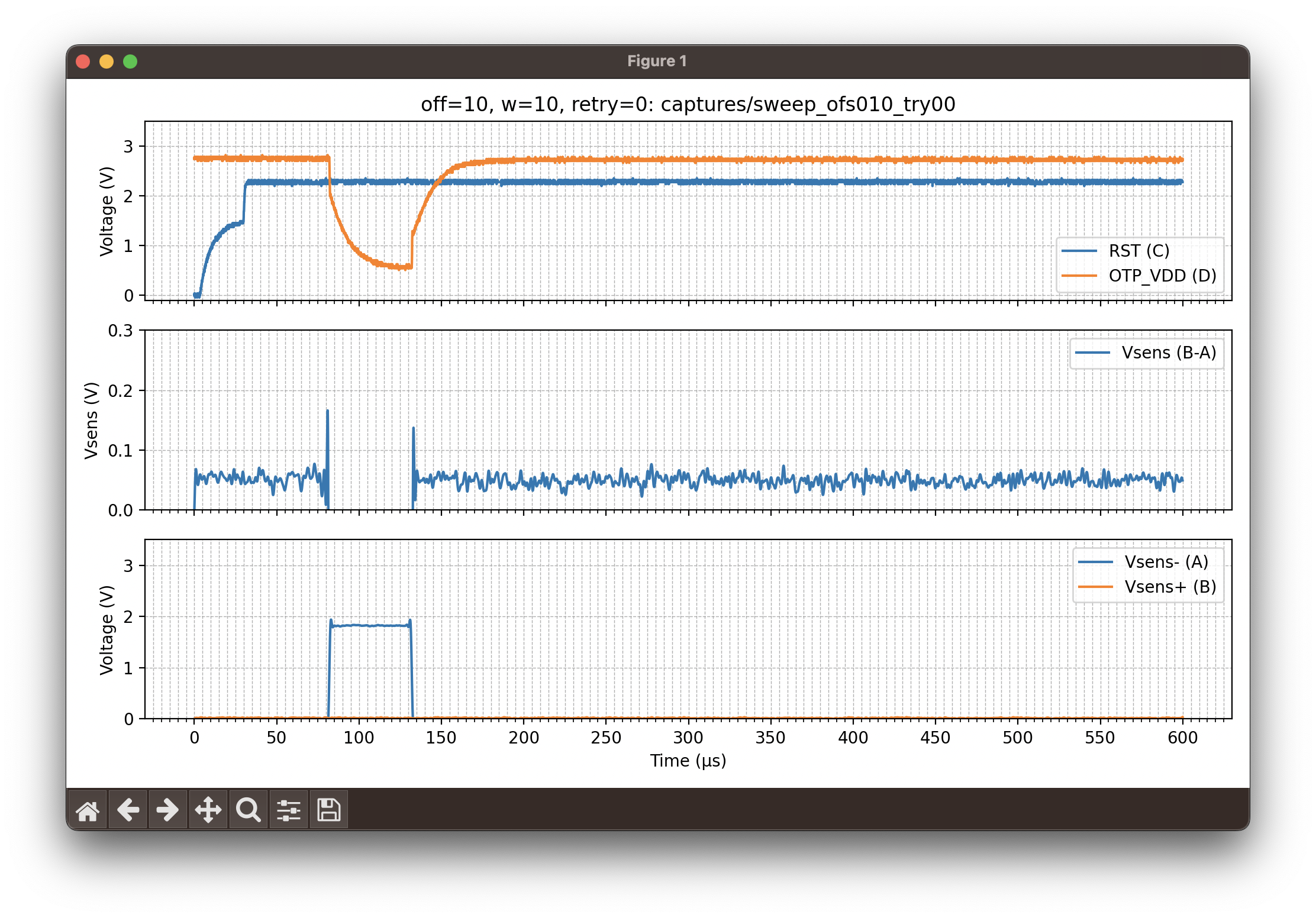
OK, now that we have the target and the current-measuring device, let’s test some captures of the OTP_VDD current draw. What are we looking for? What does the current pattern look like when the RP2350 is booting and reading critical registers from the OTP?
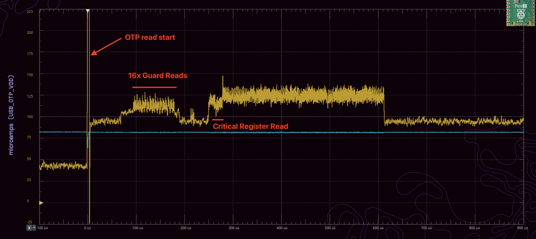
The first spike marks when the OTP reads start. After that, it is said 16 guard reads are done prior to reading the critical register to protect against power faults.
But when I did my first current captures, I got a plot like the one shown below.
The current was steady at around 30 μA (from the miniCurrent mV/μA scale), not changing over time. What is happening—where are the OTP reads? This got me stuck for a while again. Is the miniCurrent working as expected? I tested it outside this circuit and it seemed to be working. Am I connecting it incorrectly? I started forming multiple hypotheses about what could be wrong.
I was capturing around the same window as Aedan (~600 μs). Then I did something very basic: I extended the capture time a bit. Still nothing—everything was static, no signs of OTP consumption! 🤔
The Missing 1.4ms
By chance, one day I extended even more—to 1 ms, then 2 ms of capture—and bingo, there it was!
The explanation for the delay is that Aedan’s captures are shown from his trigger point, so they do not show the time from when the target is reset. I had overlooked Aedan’s Hacking the RP2350 repository, where he says:
(…) Just drop USB_OTP_VDD for 50 μs or so across the CRIT0 and CRIT1 OTP PSM reads, which on my chips are around 220-250 μs from the characteristic current spike that marks the beginning of the OTP PSM sequence. (I trigger my scope on that spike.)
My trigger was being set from the reset signal instead. So either I had to delay the capture by ~1.4 ms or use a different trigger configuration.
So far this is what was done:
- The RP2350 target was prepared to allow capturing the OTP_VDD current (and also to glitch it when the glitching circuit was ready);
- The current-measuring circuit is working;
- The OTP reads were located (~1.4 ms from reset);
Next I will explain how I decided to control the target power.
Target Control
The attack requires glitching the OTP_VDD right after the RP2350 is powered, during boot. Glitching is not deterministic, so we need to try multiple times. Hence, we need a way to programmatically control the target: start it and turn it off.
A simple way to control the target is through the RUN pin which can be seen as the reset signal. In case of RP2350, we pull it down to ground to turn off the chip. If it’s unconnected, it will be high due to the internal pull-up, thus in running mode.
My PicoScope doesn’t have digital outputs, but it does have an AWG which can be used for the glitching signal (more about this below). So I used another Pico 2 board to control the target. I wrote basic code that provides a prompt and, using short commands, turns the target on for a period of time. By default, the target-control pin output is low to keep the target turned off.
Since the RUN pin is pulled up internally, our target-control signal must have two states: high impedance (RP2350 active) or low (to turn the RP2350 off). Otherwise we create a VDD loop. It probably isn’t harmful given the low voltage/current in the loop, but if we can avoid it, why not.
void set_target_off(void) {
  gpio_put(reset_gpio, 0); // set output LOW
  gpio_set_dir(reset_gpio, GPIO_OUT); // set direction out
}

void set_target_on(void) {
	// Set pin in high-impedance (input direction)
	gpio_set_dir(reset_gpio, GPIO_IN);
}
The other relevant code runs when the target-control Pico 2 receives a command from the host to switch the target on. The command is o [<us_delay>] where the delay is the time the target will continue running after the reset. By default, it’s 5 seconds.
void handle_on_command(char *buf)
{
  unsigned int timeout = DEFAULT_TIMEOUT_US;
  if (sscanf(buf + 2, "%u", &timeout) == 1) {
    printf("[glitcher] Timeout set to %u microseconds.\n", timeout);
  } else {
    printf("[glitcher] Using default timeout of %u microseconds.\n",
    DEFAULT_TIMEOUT_US);
  }

  set_target_on();

  // Cancel any existing alarm
  if (timeout_alarm_id > 0) {
    cancel_alarm(timeout_alarm_id);
  }

  // Set a new alarm for the timeout
  timeout_alarm_id = add_alarm_in_us(timeout, timeout_callback, NULL, false);
  printf("[glitcher] Alarm set for %u microseconds.\n", timeout);
}
The timeout_callback simply calls the set_target_off function.
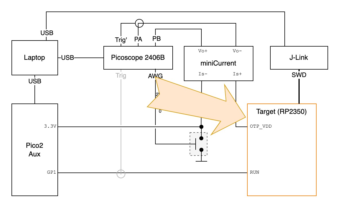
Glitching Signal
The glitching signal controls when the OTP_VDD glitch should happen. The goal is to place the glitch with microsecond precision when the CRITICAL register is read, as shown below.
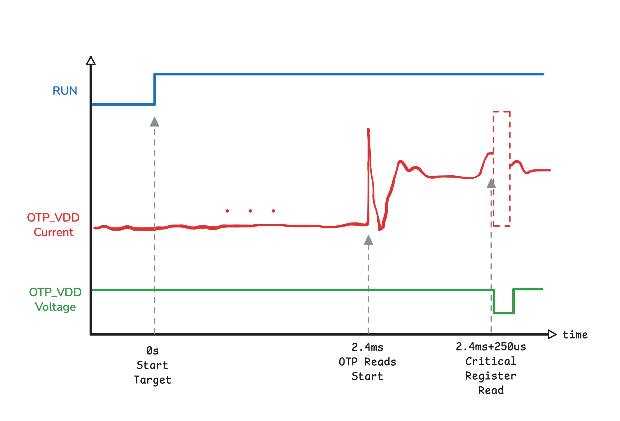
We need a way to precisely control the timing of the glitch relative to another signal and to move it in 5 μs steps, because we don’t know the exact time the glitch should occur, so we sweep it over a specific range until it succeeds.
The Analog Discovery 2 used by Aedan has a digital output pin that he used as a power source to precisely inject the glitch, which is very convenient. My PicoScope doesn’t have that digital output, but it does include an Arbitrary Waveform Generator (AWG) which could be used for the same purpose—if not for the following limitations:
- The AWG output is limited to ~3.3 mA, and
- The AWG output maximum voltage is 2 V.
I need 3.3 V to feed the OTP_VDD! Even if the AWG could supply 3.3 V, for a 50 μs glitch and a load of ~20 nF (roughly measured OTP_VDD capacitance) with a 3.3 mA drive strength, the rise/fall time would be ~36 μs—so generating a clean 50 μs glitch would be impractical (best case a glitch of ~72 μs).
There’s nevertheless one key feature from the AWG: precise control of a square pulse. I can create a 50us pulse an move it around with high precision. However, I will need to add an external circuit (i.e., like a buffer) to handle the OTP_VDD capacitive load.
While experimenting, I found that the AWGs are actually quite versatile. For example, an AWG signal can be configured to start only at a specific trigger, and it’s possible to generate a signal based on a binary sequence. It was a scope feature I had not used before, so I thought it was a good opportunity to learn more about it.
For example, if I configure the AWG so that each bit takes 5 μs and use the following waveform:
1 1 1 1 0 0 0 0 0 0 0 0 0 0 1 1 1 1 1...
It will generate a signal that is high for 4×5 μs, low for 10×5 μs, and high again. The official PicoScope Python SDK is not very practical (it’s like a direct binding to the C code), so I used Collin’s PicoScope Python library (this is changing, though). I created a basic script to programmatically change the sequence and, in this case, shift where the signal drop starts.
The relevant code snippets are the following.
(...)
AWG_N = 512
(...)
awg_freq = int(781/2)
log(f"AWG frequency set to {awg_freq} Hz")
deltaPhase = ps.getAWGDeltaPhase(awg_freq, indexMode=0, bufferLength=AWG_N)
(...)
wave = build_drop_wave(low_bits, ofs, 0, mx, AWG_N, inverted=...)
(...)
ps.setSigGenArbitrary(
    waveform=wave,
    deltaPhase=deltaPhase,
    offsetVoltage=0,
    pkToPk=2.0,
    indexMode=0,
    shots=1,
    triggerType=ps.SIGGEN_TRIGGER_TYPES.get('Rising', 0),
    triggerSource=ps.SIGGEN_TRIGGER_SOURCES.get('ScopeTrig', 1)
)
(...)
...
I set the AWG trigger to be the same as the scope trigger. This means that when the scope triggers, the AWG will output the waveform once shortly after. The build_drop_wave function generates the wave bitstream, shown below.
def build_drop_wave(low_bits: int, offset: int, mn: int, mx: int,
  n: int = AWG_N, inverted: bool = False) -> np.ndarray:
    if not inverted:
        w = np.full(n, mx, dtype=np.int16)
        if low_bits > 0:
            for k in range(low_bits):
                w[(offset + k) % n] = np.int16(mn)
    else:
        # Inverted: baseline low and insert a HIGH pulse
        w = np.full(n, mn, dtype=np.int16)
        if low_bits > 0:
            for k in range(low_bits):
                w[(offset + k) % n] = np.int16(mx)
    return w
So, let’s recap what we have so far.
- The RP2350 target was prepared to allow capturing OTP_VDD current (and also to glitch it when the glitching circuit was ready);
- The current-measuring circuit is working;
- The OTP reads were located (~1.4 ms from reset);
- A target-control Pico 2;
- A glitching signal that drops at a configurable time after target reset.
Now we’re just missing two things:
- The glitching buffer/driver
- The attack “orchestrator” — a script that connects the different pieces (configuring the glitch signal, sweeping, resetting the target via the additional Pico 2) and executes the attack.
Let’s continue with the glitching circuit.
Glitching Circuit
The glitching circuit in this case is one that makes OTP_VDD voltage drop to zero very quickly. To create this glitching circuit, I tried to make use of an old assorted kit of BJT transistors I have. The kit has some classic transistors such as the 2N2222, and 2N3904 (NPN), 2N3906 (PNP), among others.
I did some quick searches on the internet for BJT inverter and buffer circuits. The first circuit I came across was the following.
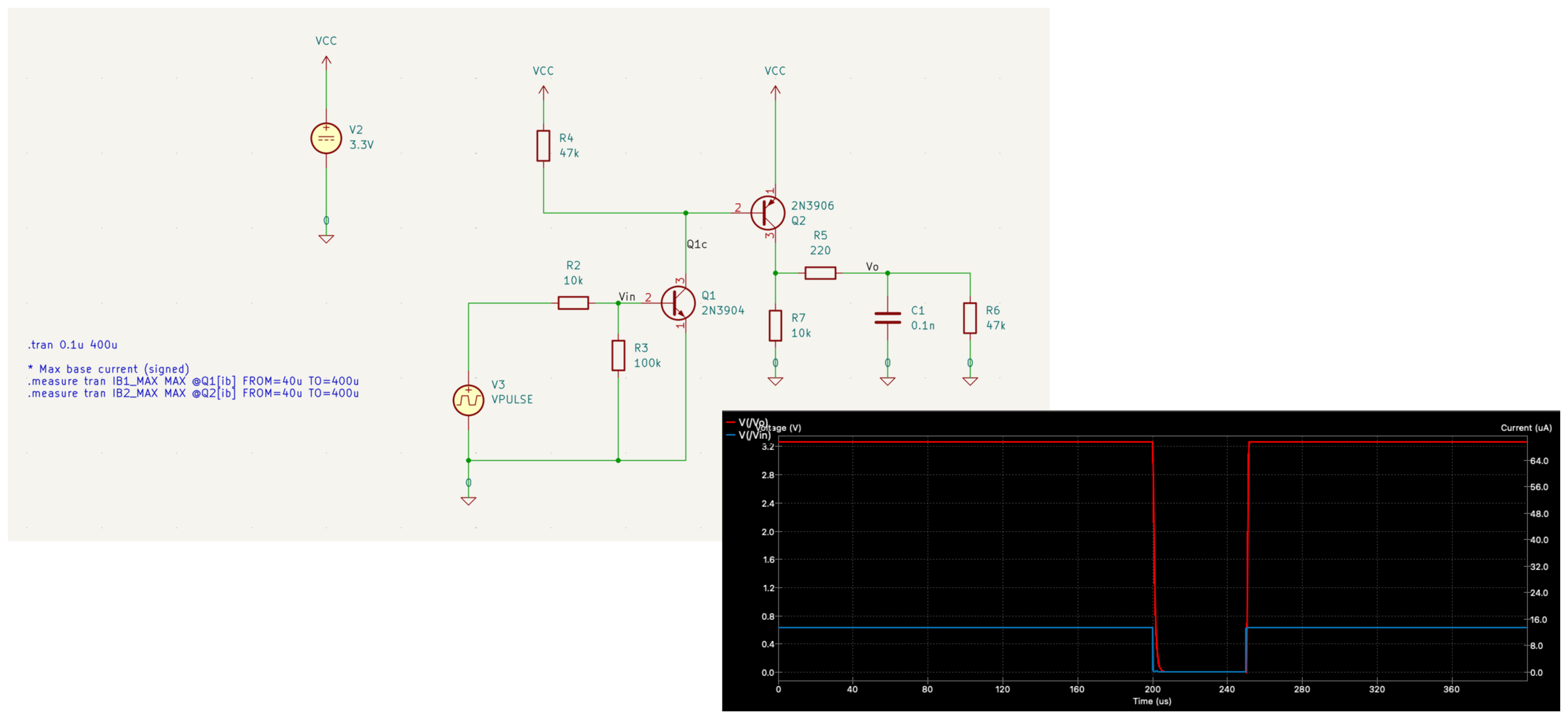
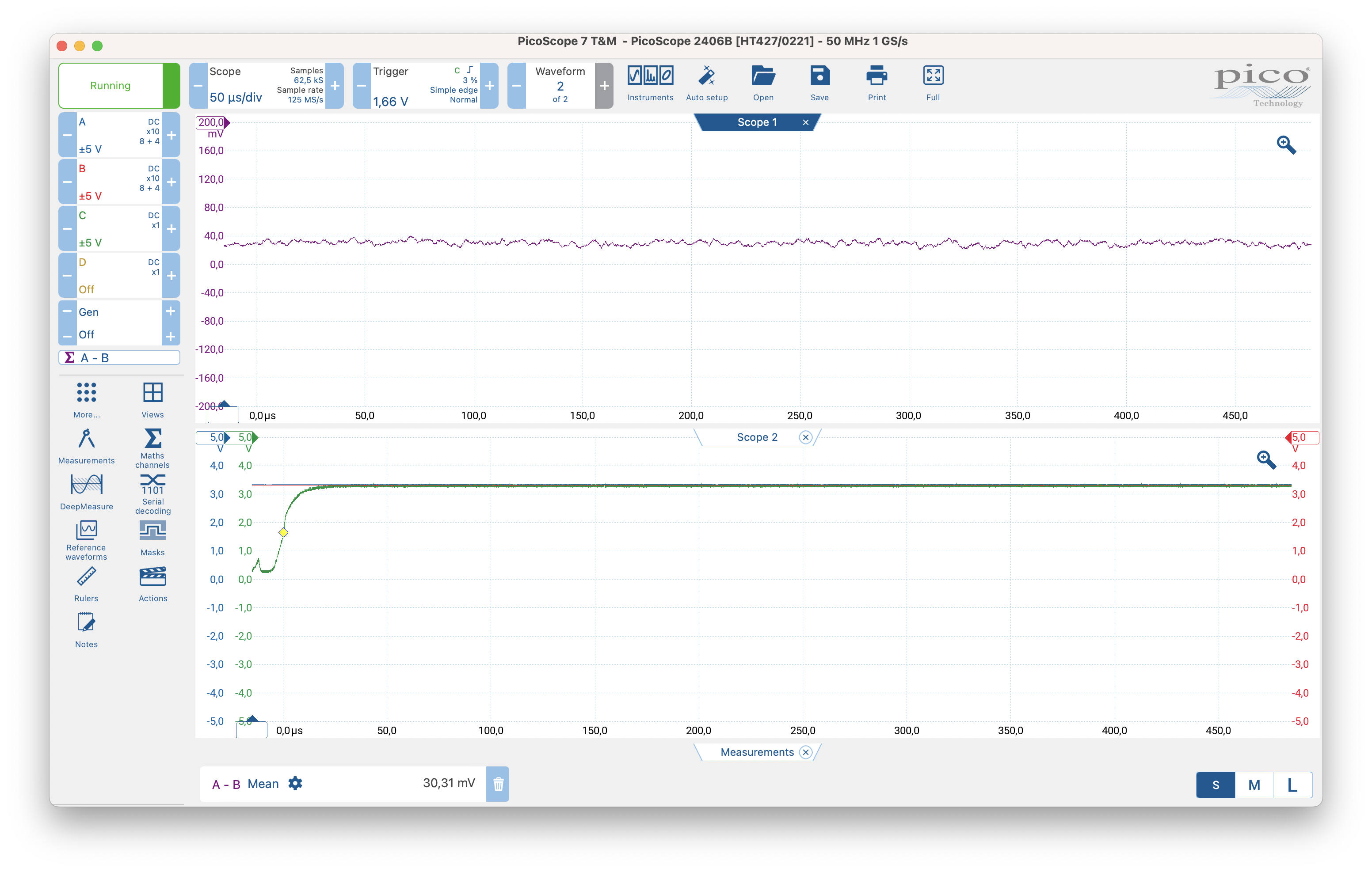
The simulation looked promising… let’s see in reality. First I assembled the circuit on a breadboard as shown below.
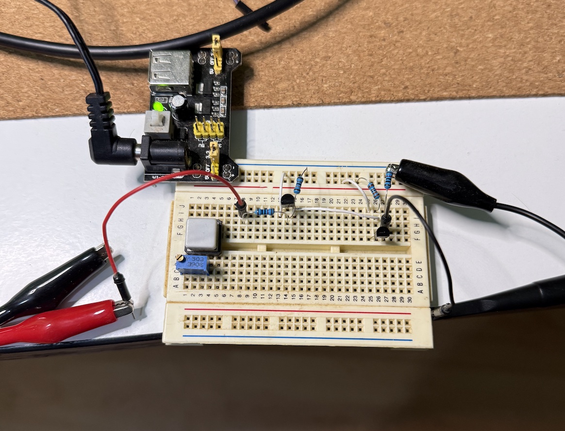
Then using my Picoscope and triggering the glitch with a switch, I captured the voltage drop I could get with this circuit.
Well, not so great; I was expecting a steep drop to zero, hold for 50 μs, then rise again to 3.3 V. Looking at the voltage drop on OTP_VDD we can see a damping effect from the capacitive load instead of a quick drop. This means I didn’t properly model my load (C1 and R6 in the schematic). Taking two points from this damping curve and fitting an RC discharge formula gives a capacitance of ~19 nF, compared to the 0.1 nF I used in the model — a big difference.
I tried multiple adjustments and different BJT circuits but couldn’t make them work for this purpose. At that point I had to decide whether to continue or go for plan B: buy a power-switch NMOS, which would simplify the design. I chose plan B, but the analog-design challenge was interesting, so I decided to revisit it after the RP2350 experiment.
I chose to buy the IRLML2502TRPBF in an SOT23 package and some SOT23-to-DIP adapter boards from AliExpress (~5€ for 20 transistors + adapters including shipping).
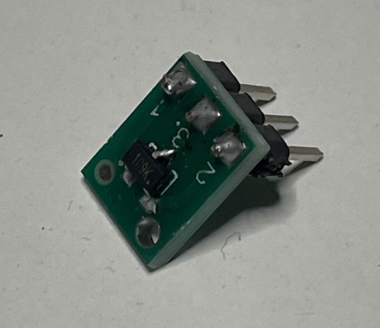
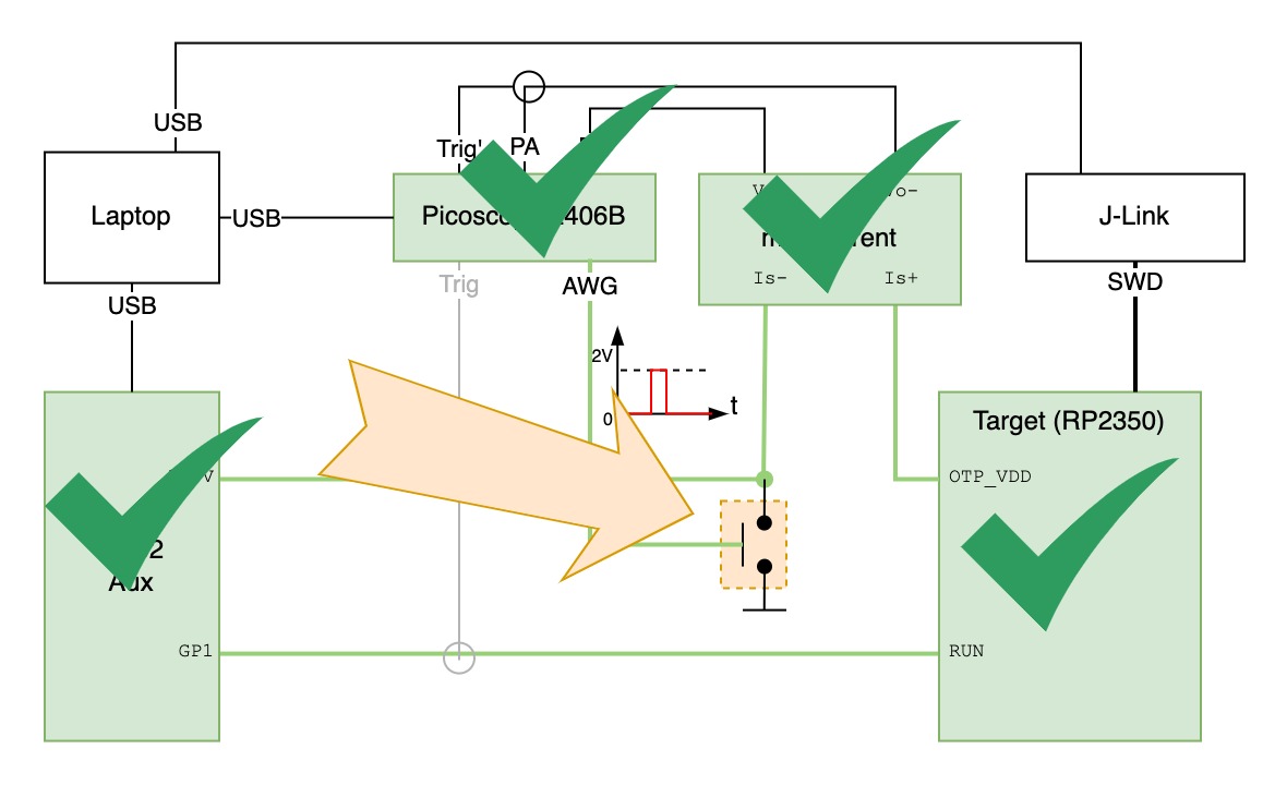
The way to connect the glitching circuit is simply connecting the gate to the trigger signal (AWG output) and the drain to the OTP_VDD, as illustrated below.
Doing the same capture that I did previously, it looks like the following.
Much better. The NMOS can drop the OTP_VDD very quickly; while recharge is slower, I can reduce the pulse width to get closer to a 50 μs pulse.
Automation & Orchestrator
Now that we have all the hardware elements, we need the attack orchestrator on the host. This can be a simple Python script that initializes the hardware and sweeps the glitch until we hit a successful event that causes the RP2350 to boot the RISC-V.
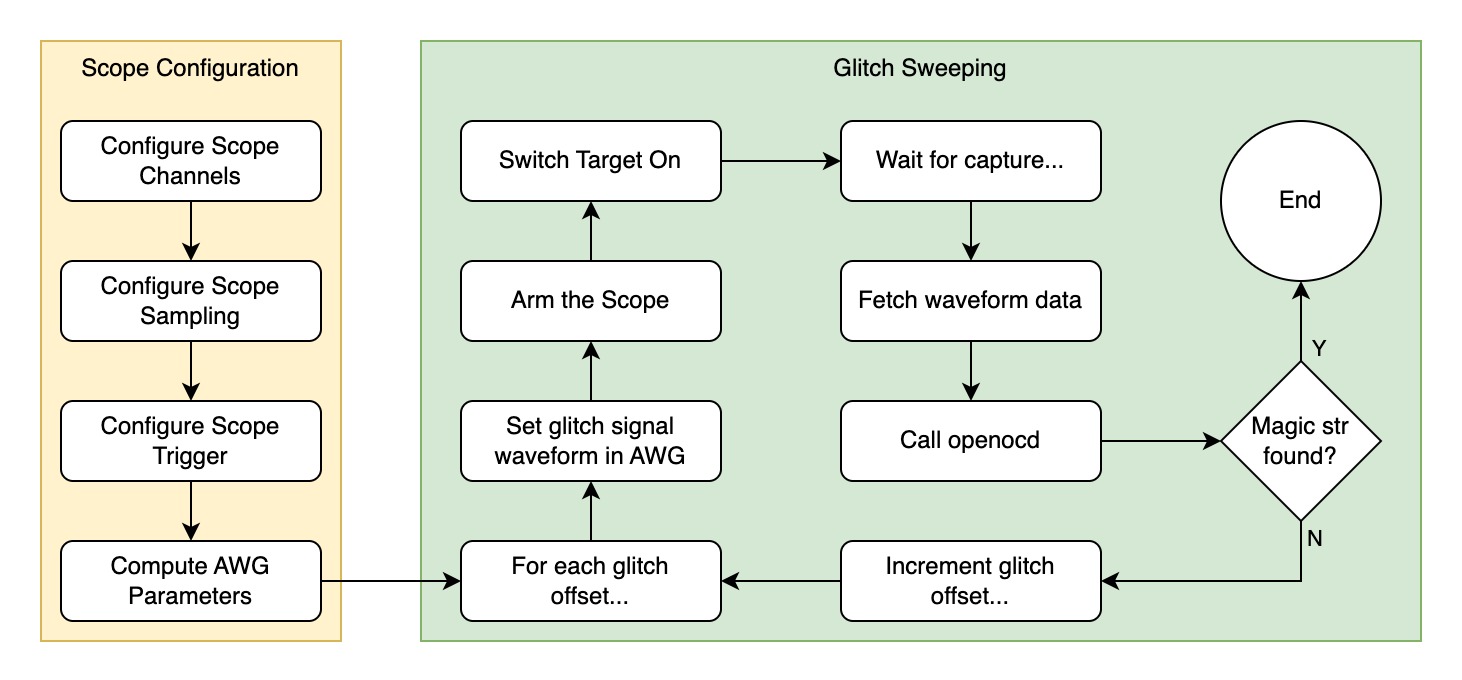
An example attack command looks like this:
python pico-otp-glitcher.py --start 320 --end 340 --trigger-delay-us 1400 \
--bw-cutoff-hz 250e3 --samples 10000 --duration 1000 --retries 20 \
--serial-port /dev/tty.usbmodem143201 --awg-pkpk 4 \
--drop-inverted --low-bits 2
The full code is shared at the end of the post.
Debugging & Failed Attempts
The first attempts at the glitch sweep did not produce any interesting effects. My earliest attempts used the BJT-based glitcher, before I had the NMOS device. The results are shown in the animation below.
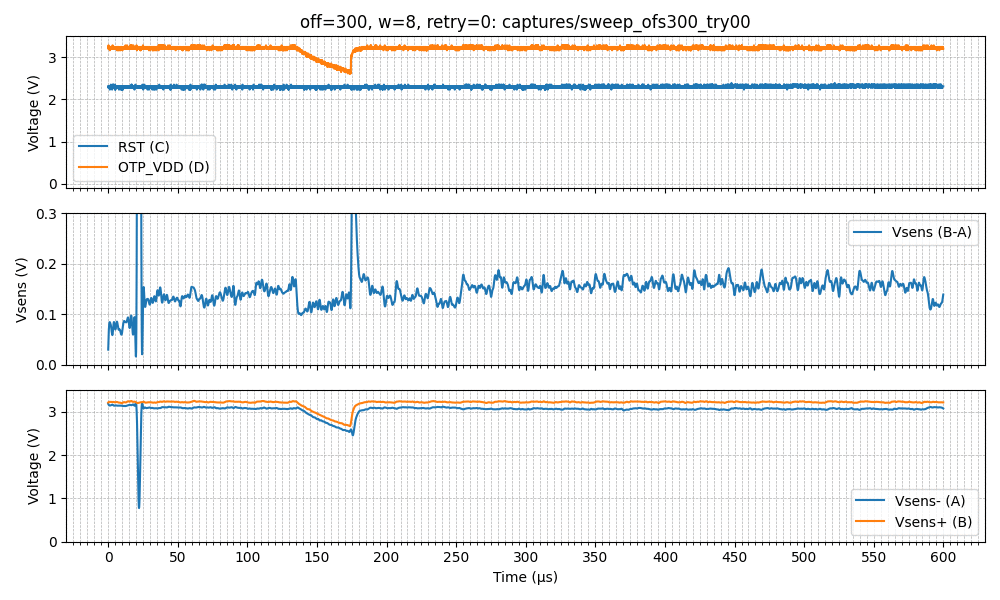
During this capture I did not see any effect on the target. The OpenOCD outputs were saved for every capture. For example:
$ cat sweep_ofs300_try06.txt
=== STDOUT ===
(no stdout)

=== STDERR ===
Open On-Chip Debugger 0.12.0+dev-00002-gcd4873400 (2025-09-12-12:57)
Licensed under GNU GPL v2
For bug reports, read
	http://openocd.org/doc/doxygen/bugs.html
Warn : Transport "swd" was already selected
Info : [rp2350.cm0] Hardware thread awareness created
Info : [rp2350.cm1] Hardware thread awareness created
ocd_process_reset_inner
Warn : An adapter speed is not selected in the init scripts. OpenOCD ...
Warn : To remove this warnings and achieve reasonable communication ...
Info : J-Link V9 compiled Sep  1 2016 18:29:50
Info : Hardware version: 9.60
Info : VTarget = 3.269 V
Info : clock speed 100 kHz
Info : SWD DPIDR 0x4c013477 DPv3
Info : [rp2350.cm0] Cortex-M33 r1p0 processor detected
Info : [rp2350.cm0] target has 8 breakpoints, 4 watchpoints
Info : [rp2350.cm0] Examination succeed
Info : [rp2350.cm1] Cortex-M33 r1p0 processor detected
Info : [rp2350.cm1] target has 8 breakpoints, 4 watchpoints
Info : [rp2350.cm1] Examination succeed
Info : [rp2350.cm0] starting gdb server on 3333
Info : Listening on port 3333 for gdb connections


=== RETURN CODE: 0 ===
Comparing all outputs, I saw no differences in the size of the OpenOCD outputs. Nothing interesting.
...
-rw-r--r--  1 jemos  staff  1246 Oct 21 23:00 sweep_ofs336_try00.txt
-rw-r--r--  1 jemos  staff  1246 Oct 21 23:00 sweep_ofs336_try01.txt
-rw-r--r--  1 jemos  staff  1246 Oct 21 23:00 sweep_ofs336_try02.txt
-rw-r--r--  1 jemos  staff  1246 Oct 21 23:00 sweep_ofs336_try03.txt
-rw-r--r--  1 jemos  staff  1246 Oct 21 23:00 sweep_ofs336_try04.txt
-rw-r--r--  1 jemos  staff  1246 Oct 21 23:00 sweep_ofs336_try05.txt
-rw-r--r--  1 jemos  staff  1246 Oct 21 23:00 sweep_ofs336_try06.txt
-rw-r--r--  1 jemos  staff  1246 Oct 21 23:00 sweep_ofs336_try07.txt
-rw-r--r--  1 jemos  staff  1246 Oct 21 23:00 sweep_ofs336_try08.txt
-rw-r--r--  1 jemos  staff  1246 Oct 21 23:00 sweep_ofs336_try09.txt
-rw-r--r--  1 jemos  staff  1246 Oct 21 23:00 sweep_ofs337_try00.txt
-rw-r--r--  1 jemos  staff  1246 Oct 21 23:00 sweep_ofs337_try01.txt
-rw-r--r--  1 jemos  staff  1246 Oct 21 23:00 sweep_ofs337_try02.txt
-rw-r--r--  1 jemos  staff  1246 Oct 21 23:00 sweep_ofs337_try03.txt
-rw-r--r--  1 jemos  staff  1246 Oct 21 23:00 sweep_ofs337_try04.txt
-rw-r--r--  1 jemos  staff  1246 Oct 21 23:01 sweep_ofs337_try05.txt
-rw-r--r--  1 jemos  staff  1246 Oct 21 23:01 sweep_ofs337_try06.txt
-rw-r--r--  1 jemos  staff  1246 Oct 21 23:01 sweep_ofs337_try07.txt
-rw-r--r--  1 jemos  staff  1246 Oct 21 23:01 sweep_ofs337_try08.txt
-rw-r--r--  1 jemos  staff  1246 Oct 21 23:01 sweep_ofs337_try09.txt
...
Then I made some adjustments to the BJT glitcher to try to improve it.
Another circuit, another try:
OK, then I got the NMOS power transistor and improved the glitching circuit. The first capture looked like this:
However, with the NMOS I started to get some glitches. The OpenOCD outputs started to vary in some random offsets:
$ /bin/ls -l *.txt | grep -v 2308
-rw-r--r--  1 jemos  staff   824 Jan 14 21:58 sweep_ofs322_try08.txt
-rw-r--r--  1 jemos  staff  2507 Jan 14 21:58 sweep_ofs323_try02.txt
-rw-r--r--  1 jemos  staff  1350 Jan 14 21:59 sweep_ofs324_try06.txt
-rw-r--r--  1 jemos  staff  2384 Jan 14 21:59 sweep_ofs325_try02.txt
...
The output had for example:
...
Info : clock speed 4000 kHz
Info : SWD DPIDR 0x4c013477 DPv3
Info : SWD DPIDR 0x4c013477 DPv3
Error: Failed to read memory at 0xe000ed00
Error: [rp2350.cm0] Execution of event check-availability failed:
...
At some point I realized I could be doing one thing wrong. Aedan’s slides show he used the J-Link Windows binary; that J-Link software behaves differently from OpenOCD. From what I understand, OpenOCD will not enumerate TAP devices — it tries to connect to the device specified in the configuration. That means you must tell OpenOCD whether to expect the ARM or the RISC-V processor. If the attack succeeds but I run OpenOCD with the ARM configuration, OpenOCD will fail, and it won’t be clear whether the failure was due to a bad glitch or because the device actually booted the RISC-V.
Thus, I had to change the OpenOCD command to assume the RISC-V was booted instead. The command is:
# Old
./openocd -s tcl -f interface/jlink.cfg -c "transport select swd" \
-f "target/rp2350.cfg" -c "init; targets; exit"

# New
./openocd -s tcl -f interface/jlink.cfg -c "transport select swd" \
-f "target/rp2350_riscv.cfg" -c "init; targets; exit"
With this change the outputs looked like this:
...
Info : [rp2350.rv0] datacount=1 progbufsize=2
Info : [rp2350.rv0] unavailable.
Error: [rp2350.rv0] Examination failed
Warn : target rp2350.rv0 examination failed
...
It wasn’t working… Sweeping the glitch did not cause it to boot the RISC-V. There were some changes in the output, but not the result I was looking for.
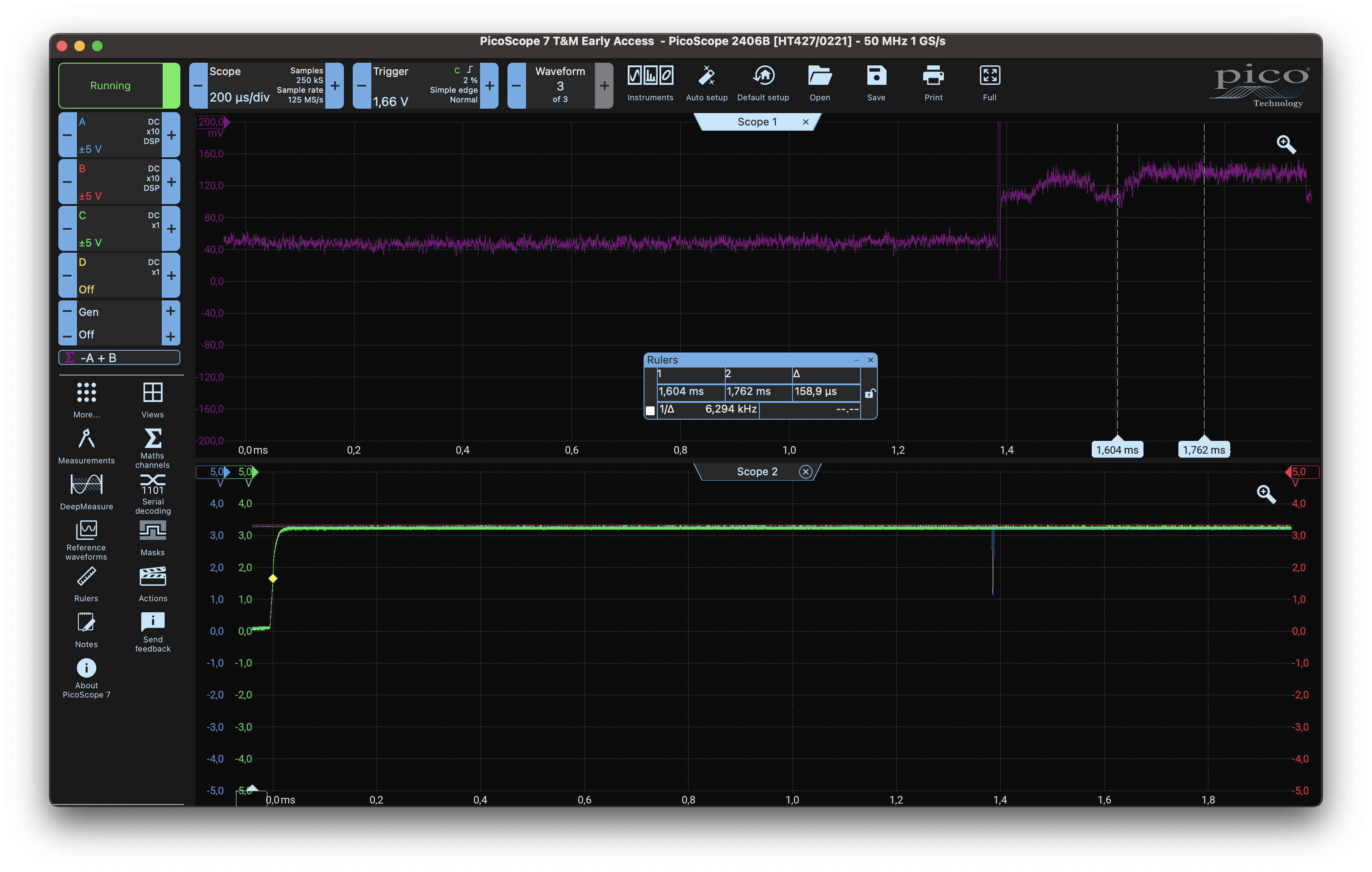
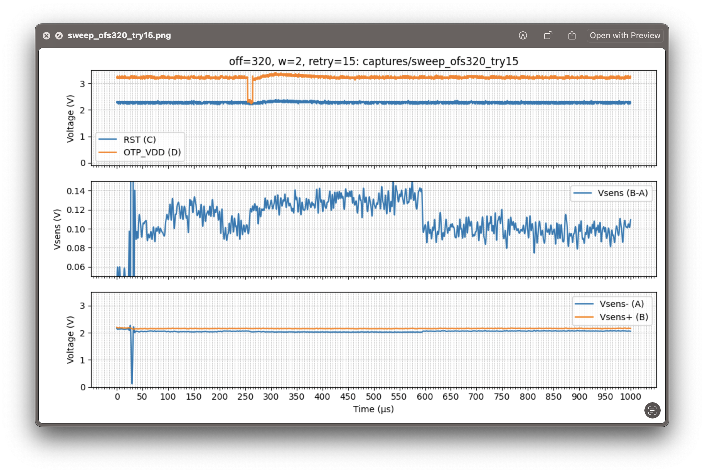
The Real Problem: Jitter
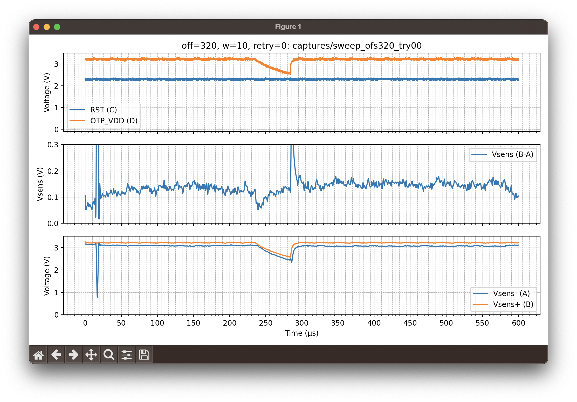
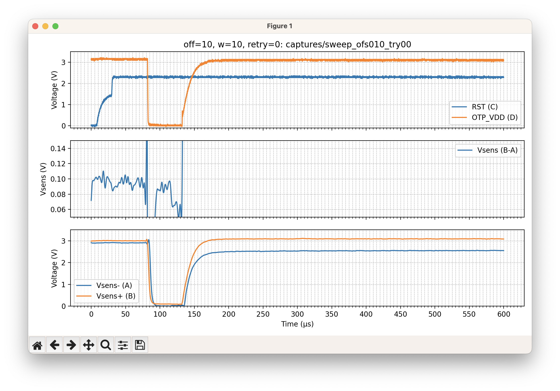
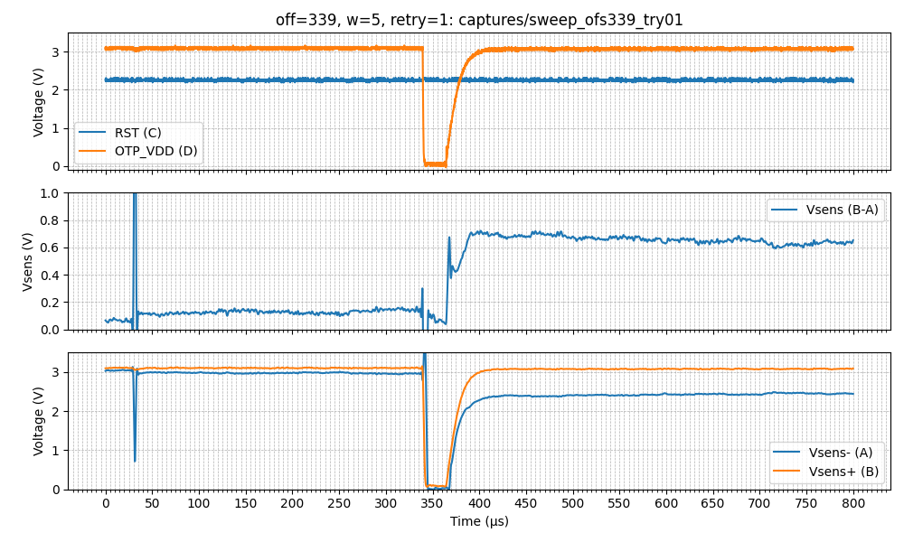
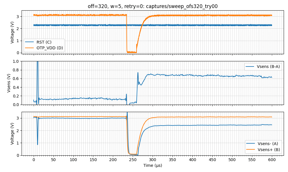
Until now, I had been using a reset-based trigger. When the target resets, that’s when the timer starts counting to schedule the glitch. The glitch happens ~1.4 ms + 250 μs after reset. Look at the following capture and notice how the blue spike (when OTP reads start) and the glitch (orange signal drop) are not aligned across different retries for the same glitch offset (off=334, 335, etc.). As shown, there was noticeable jitter; the interval between the OTP read start and the glitch did not shift smoothly — it moved back and forth.
Initially I overlooked this. I assumed that by shifting the glitch it would eventually hit the right time, even with jitter. The final step to make this attack work was to use the same glitch trigger as Aedan’s: the OTP-read-start spike.
I configured the scope trigger for a rising edge crossing 1.51 V on probe A. The result is shown below.
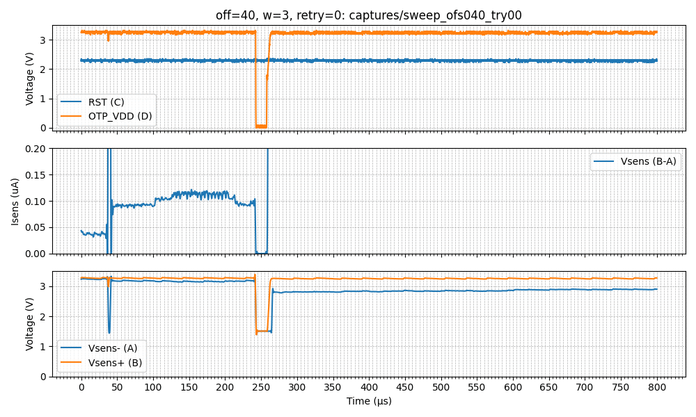
The glitch now shifts in a much more consistent way. I reduced the pulse width to ~35–40 μs because the rising and falling edges were not sharp.
That was the turning point. After reaching offsets 46–47, the glitch caused the RP2350 to boot the RISC-V!
$ python pico-otp-glitcher.py --start 46 --end 47 --bw-cutoff-hz 500e3 --samples 10000 \
--duration 800 --retries 10 --serial-port /dev/tty.usbmodem143301 --awg-pkpk 4 \
--drop-inverted --low-bits 3

[2026-01-25 23:50:57.540] Opening PicoScope 2000A...
[2026-01-25 23:51:01.273] Configuring channels A, B, C, D: DC, ±5V
[2026-01-25 23:51:01.274] Requesting a sampling period of 0.080 µs for a total duration of 800.0 µs
[2026-01-25 23:51:01.276] Sampling interval set: dt=0.72us, samples=11111 (max 8388585), pretrig=5%
[2026-01-25 23:51:01.276] Setting trigger on A rising at 0V (scope)
[2026-01-25 23:51:01.277] AWG code range unavailable, using int16 fullscale
[2026-01-25 23:51:01.277] Sweep offsets: start=46, end=47, low_bits=3, drop_inverted=True
[2026-01-25 23:51:01.277] AWG frequency set to 390 Hz
Calculated deltaPhase for 390 Hz: 1309 (capdur=8.0e-04s, n=512)
[2026-01-25 23:51:01.278] Building waveform for offset 46
[2026-01-25 23:51:01.280] Wave: (...)
[2026-01-25 23:51:01.281] Programming AWG for offset 46
[2026-01-25 23:51:06.289] Offset 46: capture 1/10
[2026-01-25 23:51:06.290] Running block capture (arming scope)...
[2026-01-25 23:51:06.454] Sending trigger to Pico2...
[2026-01-25 23:51:06.454] Opening serial port /dev/tty.usbmodem143301 @ 115200 baud...
[2026-01-25 23:51:06.673] [glitcher] Sending 'off' command first to clear previous on state.
[2026-01-25 23:51:06.674] [glitcher] Sending 'on' command with timeout 600000000 us...
[2026-01-25 23:51:06.674] [glitcher] Waiting for response...
[2026-01-25 23:51:06.679] [glitcher] Responded with: b'f'
[2026-01-25 23:51:06.683] [glitcher] Responded with: b'[glitcher] Target manually turned off.'
[2026-01-25 23:51:06.683] [glitcher] Responded with: b'> o 600000000'
[2026-01-25 23:51:06.684] [glitcher] Responded with: b'[glitcher] Timeout set to 600000000 microseconds.'
[2026-01-25 23:51:06.685] [CHECK] Response contains expected line: PASS
[2026-01-25 23:51:06.689] Fetching data from scope...
[2026-01-25 23:51:21.093] Running OpenOCD for capture and writing output to captures/sweep_ofs046_try00.txt
RISC-V core booted... try to connect to it via gdb...
Now I launch OpenOCD manually to open a GDB port:
Open On-Chip Debugger 0.12.0+dev-00002-gcd4873400 (2025-09-12-12:57)
Licensed under GNU GPL v2
For bug reports, read
	http://openocd.org/doc/doxygen/bugs.html
Warn : Transport "swd" was already selected
Info : [rp2350.rv0] Hardware thread awareness created
Info : [rp2350.rv1] Hardware thread awareness created
ocd_process_reset_inner
Info : J-Link V9 compiled May  7 2021 16:26:12
Info : Hardware version: 9.60
Info : VTarget = 3.262 V
Info : clock speed 100 kHz
Info : SWD DPIDR 0x4c013477 DPv3
Info : [rp2350.rv0] datacount=1 progbufsize=2
Info : [rp2350.rv0] Disabling abstract command reads from CSRs.
Info : [rp2350.rv0] Disabling abstract command writes to CSRs.
Info : [rp2350.rv0] Core 0 could not be made part of halt group 1.
Info : [rp2350.rv0] Examined RISC-V core
Info : [rp2350.rv0]  XLEN=32, misa=0x40901105
Info : [rp2350.rv0] Examination succeed
Info : [rp2350.rv1] datacount=1 progbufsize=2
Info : [rp2350.rv1] Disabling abstract command reads from CSRs.
Info : [rp2350.rv1] Disabling abstract command writes to CSRs.
Info : [rp2350.rv1] Core 1 could not be made part of halt group 1.
Info : [rp2350.rv1] Examined RISC-V core
Info : [rp2350.rv1]  XLEN=32, misa=0x40901105
Info : [rp2350.rv1] Examination succeed
Info : [rp2350.rv0] starting gdb server on 3333
Info : Listening on port 3333 for gdb connections
    TargetName         Type       Endian TapName            State
--  ------------------ ---------- ------ ------------------ ------------
 0* rp2350.rv0         riscv      little rp2350.cpu         running
 1  rp2350.rv1         riscv      little rp2350.cpu         running
Info : Listening on port 6666 for tcl connections
Info : Listening on port 4444 for telnet connections
Info : accepting 'gdb' connection on tcp/3333
rp2350.rv0 halted due to debug-request.
rp2350.rv1 halted due to debug-request.
Info : RP2350 rev 2, QSPI Flash win w25q128fv/jv id = 0x1840ef
size = 16384 KiB in 4096 sectors
Info : New GDB Connection: 1, Target rp2350.rv0, state: halted
Finally, with a GDB that supports the RISC-V architecture, we connect to the OpenOCD session and read the OTP secrets at the memory-mapped address 0x40137020:
$ riscv64-elf-gdb
GNU gdb (GDB) 17.1
Copyright (C) 2025 Free Software Foundation, Inc.
License GPLv3+: GNU GPL version 3 or later <http://gnu.org/licenses/gpl.html>
This is free software: you are free to change and redistribute it.
There is NO WARRANTY, to the extent permitted by law.
Type "show copying" and "show warranty" for details.
This GDB was configured as "--host=x86_64-apple-darwin22.6.0 --target=riscv64-elf".
Type "show configuration" for configuration details.
For bug reporting instructions, please see:
<https://www.gnu.org/software/gdb/bugs/>.
Find the GDB manual and other documentation resources online at:
    <http://www.gnu.org/software/gdb/documentation/>.

For help, type "help".
Type "apropos word" to search for commands related to "word".
(gdb) set remotetimeout 60
(gdb) target remote localhost:3333
Remote debugging using localhost:3333
⚠️ warning: No executable has been specified and target does not support
determining executable automatically.  Try using the "file" command.
0x00007640 in ?? ()
(gdb) x/32wx 0x40137020
0x40137020:	0x0022c0ff	0x0014ffee	0x0022c0ff	0x0014ffee
0x40137030:	0x0022c0ff	0x0014ffee	0x0022c0ff	0x0014ffee
0x40137040:	0x00000000	0x00000000	0x00000000	0x00000000
0x40137050:	0x00000000	0x00000000	0x00000000	0x00000000
0x40137060:	0x00000000	0x00000000	0x00000000	0x00000000
0x40137070:	0x00000000	0x00000000	0x00000000	0x00000000
0x40137080:	0x00000000	0x00000000	0x00000000	0x00000000
0x40137090:	0x00000000	0x00000000	0x00000000	0x00000000
(gdb) x/1wx 0x40120148
0x40120148:	0x00030033
Conclusion
Reproducing this attack was less about generating a stronger glitch and more about understanding the system’s timing and measurement constraints. The breakthrough did not come from sharper edges or more aggressive pulses, but from choosing the right trigger and observing the system correctly.
Along the way, tooling assumptions, instrumentation limitations, and small architectural details proved just as important as the glitch circuit itself. What looked at first like hardware limitations often turned out to be measurement or synchronization problems.
This is probably obvious, but investing time (and in some cases money) in a solid hardware setup leads to smoother, more predictable experiments. For example, the custom target board to access OTP_VDD directly, eliminated the need for invasive hardware modifications (i.e., PCB reworking, cutting PCB traces).
This turned into a multi-month experiment that I pursued intermittently in my spare time. On more than one occasion, I thought about giving up. For me, the key was to resist starting something new before bringing this project to completion.
Yet the journey itself was worth it — I learned a great deal along the way.
Project Files
Note: these files were not edited for general use, they were not cleaned up. Consider them just as a referrence.
- pico-otp-glitcher.py
- pico-otp-glitcher.c
- KiCad Custom RP2350 Target Board RP-006440-DD-2-RP2350A.zip